Downloaded 4,335 times
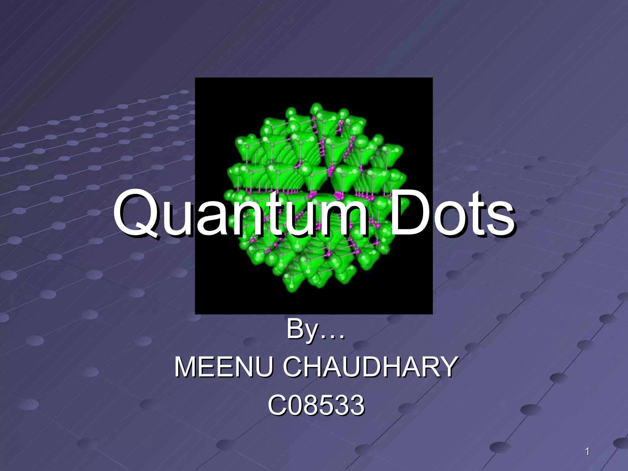


Quantum dots are semiconductor nanoparticles that confine electrons and holes in all three dimensions. They are made using different methods like lithography, colloidal synthesis, or epitaxy. Quantum dots have discrete energy levels that depend on their size and shape. They have potential applications in solar cells, LEDs, bioimaging, drug delivery, and anti-counterfeiting due to their tunable light emission properties.


